What is a flash memory chip? What are the types?
Oct 24, 2023
1. What is a flash memory chip
Flash memory chip is a hierarchical management of flash memory storage unit chip, internal structure from high to low can be expressed as: chip Package (Package)→ layer (Die)→ Block (Block)→ Page (Page)→ storage Cell (Cell). The operating unit of the memory chip is page (page), the capacity of each page is generally 4KB or 8KB, and there is an out-of-band area (Out of Band, OOB) outside the data area of the page, generally more than 128 bytes, generally used to store the metadata information and verification information of the page.
2. Type of flash memory chip
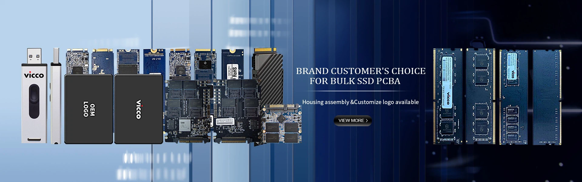
There are also different types of flash memory, which are mainly divided into NOR type and NAND type two categories.
The difference between NOR type and NAND type flash memory is very big, for example, NOR type flash memory is more like memory, there is an independent address line and data line, but the price is more expensive, the capacity is relatively small; The NAND type is more like a hard disk, the address line and the data line are shared I/O lines, and all information similar to the hard disk is transmitted through a hard disk line, and NAND type compared with NOR type flash memory, the cost is lower, and the capacity is much larger. Therefore, NOR flash memory is more suitable for frequent random read and write occasions, usually used to store program code and run directly in flash memory, mobile phone is the use of NOR flash memory, so the "memory" capacity of mobile phone is usually not large; NAND flash is mainly used to store data, and our commonly used flash products, such as flash disks and digital memory cards, are NAND flash.
3. Several working states of flash memory chip
(1) Read by page operation
The default state of the flash memory chip is read. The read operation starts by writing the 00h address to the instruction register through 4 address cycles. Once the instruction is latched, the read operation cannot be written in the next page.
You can output data randomly from a page by writing random data output instructions. The data address can be automatically found from the data address to be output by random output instructions to find the next address. Random data output operations can be used multiple times.
(2) Page programming
The programming of the flash chip is page by page, but it supports multiple partial page programming in a single page programming cycle, and the number of consecutive bytes of the partial page is 2112. Write the page programming confirmation instruction (10h) to start the programming operation, but you must also enter continuous data before writing the instruction (10h).
Continuous loading data After writing the continuous data input instruction (80h), 4 cycles of address input and data loading will begin, while the word, unlike programmed data, does not need to be loaded. The chip supports random data input in the page, and can automatically change the address according to random data input instruction (85h). Random data entry can also be used multiple times.
(3) Cache programming
Cache programming is a type of page programming that can be performed by 2112 bytes of data registers and is only valid in a block. Because the flash chip has a page cache, it can perform continuous data input when the data register is compiled into the memory unit. Cache programming can only begin after the unfinished programming cycle has ended and the data register has been transferred from the cache. The R/ B pin allows you to determine whether internal programming is complete. If the system only uses R/ B to monitor the process of the program, then the order of the last page object program must be arranged by the current page programming instruction.
(4) Storage unit replicating
This feature can quickly and efficiently rewrite data in a page without the need to access external memory. Because the time spent on continuous access and reloading is reduced, the performance of the system is improved. This is especially true when part of a block is upgraded and the rest needs to be copied into a new block. This operation is a continuous read instruction, but does not need to continuously access and copy the program to the destination address. An original page address instruction of "35h read operation can transfer the entire 2112 bytes of data into the internal data buffer." When the chip returns to the ready state, the page copy data entry instruction with the destination address loop is written. The error procedure in this operation is indicated by the "Pass/fail" status. However, if this operation takes too long to run, it will cause a bit operation error due to data loss, resulting in the failure of the external error "Check/correct" device check. For this reason, the operation should be corrected using a two-digit error.
(5) Block erase
The erase operation of flash memory chip is carried out on the basis of block. Block address loading starts with a block erase instruction and is completed in two loops. In fact, when address lines A12 to A17 are suspended, only address lines A18 to A28 are available. Load the erase confirmation instruction and block address to start erasing. This must be done in this order to avoid erasing errors from the contents of the memory affected by external noise.
(6) Read status
The status register in the flash memory chip confirms that programming and erasure operations have been successfully completed. After writing the instruction (70h) to the instruction register, the read loop outputs the contents of the status register to I/ O at the falling edge of CE or RE. The instruction register remains in the read state until a new instruction arrives, so if the status register is in the read state during a random read loop, a read instruction should be given before the read loop begins.


